Simon Frankau's blog
Electronics for Newbies: Memory Banking
So, the main piece of interest in my noddy Z80 is the memory banking, allowing it to address more than 64K at once. Back when I had a Spectrum, this seemed something like magic, and now it's a pleasure to have a go at it myself. Without further ado, here's my dodgy schematic, thanks to Eagle.
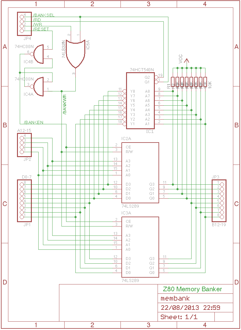
The basic idea is that each 4K chunk of memory can be mapped to one of 256 locations, bringing the total address space to one meg. All rather 8086. To make this work, we want a little memory with 4 bits of addressing (top address bits in), and 8 bits of data (top address bits out). The 74289 more or less does the job, but only has 4 bits of data, so we use two.
Labelling-wise, An is the CPU's address bus, and Bn is the segmented/paged full memory bus. A0-11 map straight to B0-11. Dn is the normal data bus. For control signals, we have /BANKSEL, which is triggered by address decoding and IO access, plus the normal /RD, /WR and /RESET.
So, how does the circuit work? Initially, ignore the Bn bus, and the control circuitry, and just look at the 74540 and 75289s. It's really just a simple memory. Select the location via the A12-15 lines, and either write or read over the data bus. The 74LS289 has inverting outputs, so we use an inverting buffer. The 74289 is only available in LS format at best (by the time they were making CMOS 74-series chips, they probably wondered why anyone would ever want such a tiny memory...), so I need to use the HCT version to buffer it. The 74289 has open collector outputs, which means that when they're disabled their output is all ones, and if you do a read through the inverting '540 you'll see zero, which is a nice initial value. I'm using 10K pull-ups because it's what I have to hand, and is in the appropriate ball-park for pull-ups.
So, what's all this about using A12-15 to control the configuration of banking, given that IN/OUT takes an 8-bit address that goes on the lower bits? Well, it doesn't really. You can actually control the high bits with the appropriate instructions (An OUT (BC), I think), which was used for example to scan the Spectrum's keyboard. Here I'm using it to massively simplify the banking logic.
Why use A12-15 to select the bank to read/write when doing I/O? Simply because when we're not doing an I/O operation to configure the banking, this circuit reads from A12-15 and writes the associated memory look-up to B12-19. In other words, it performs precisely the banking look-up we need. B12-19 are TTL level, but that's ok, 'cos it's used to drive TTL-level-supporting SRAM and EEPROM.
Now, the control circuitry. Reads happen when /BANKSEL and /RD are low. Writes happen when /BANKSEL and /RW are low (signal /BANKWR). However, on start-up the '289s may be full of random cruft, and we want to start with known EEPROM mapped in. To that effect, we have a flip-flop providing the /BANKEN signal to say whether banking is switched on or not. It is reset high be /RESET, and then enabled low by /BANKWR when data is actually written to the banking I/O address (I'm of the opinion that I/O reads should try to avoid triggering side effects, hence using /BANKRW, not /BANKSEL).
That's it in theory, and my soldering up will eventually reveal the practice. What could I have done differently? Well, I was tempted to have /BANKEN also reset upon, for example, NMI, so that the NMI could go to a monitor from a known state. A further extension could enable I/O reads to return the configuration, even if /BANKEN is off, enabling such a monitor to save down the banking state before doing its own thing and eventually restoring the state of the previously running program. However, I really want to keep the complexity and chip count down, and I suspect I'm not going to have the time to write complex software to really take advantage of such features. So, KISS. In which case, this whole thing is actually pointless overkill, but it's been fun.
Doing all this stuff feels surprisingly adventurous. I have to remind myself there are people ten years younger than myself working on the cutting edge, and pottering about with what is fundamentally retro technology is just so no big deal, but this is just a lot of fun. Despite a PhD (in hardware synthesis!) in the way, it feels pretty much like no gap from trying to build a simple ALU from vanilla 74-series chips in my teenage years (doing it all wrong, and having lots of fun...).
Posted 2013-08-23.