Simon Frankau's blog
Electronics for Newbies: Now with documentation...
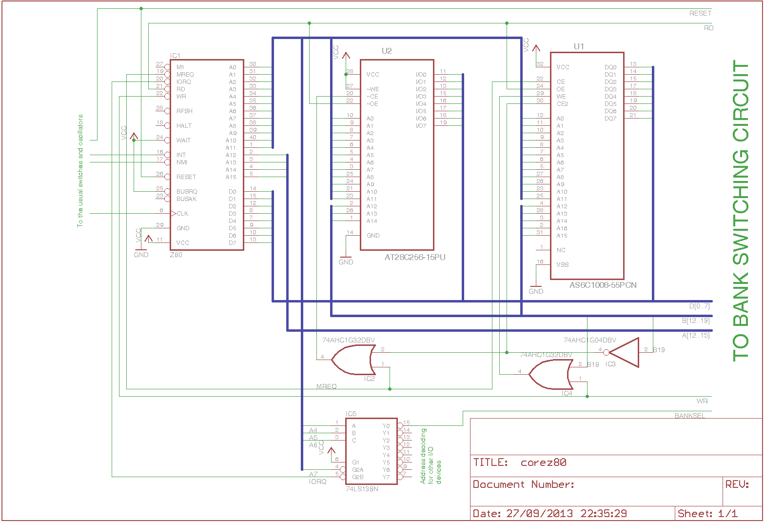
I've not made any real progress since my last Z80ing post, but I think I can still flesh out the documentation side a little. I've sketched up a loose circuit diagram for what I've built - skipping all the dull stuff like decoupling caps, and the RC reset circuit, etc.
I also have a couple of photos, of where I've got to with the PCB (see the fugly mess of wires, in rainbow organisation, see the empty space reserved for SIO etc.), and how I hooked it up to a latch and LEDs for testing...
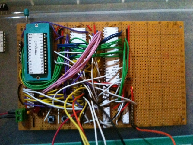
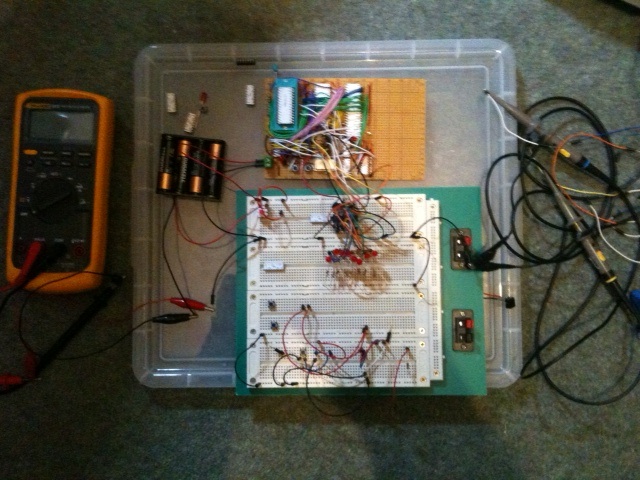
Yeah, they're a bit uninspiring and blurry, but what do you want out of a quick photo at night on an old phone?
I have written a little bit of system exerciser code, and one thing I'd rediscovered was that the chips used to do the banking have inverting memories. So, it powers up to access the memory at 0xFF000, but if you then want to map it in software, you actually want to map it from 0x00000. Or perhaps a more sane way to view it is the boot ROM is mapped at 0x00000, but the data in the EEPROM has to be juggled by shuffling all the data to flip the top eight bits of addressing.
So, taking that into account, and ignoring the fact that only partial memory addressing is done (hence much mirroring of the same address space), the 'physical' software-oriented memory map looks like the following:
- 0x00000 - 0x07FFF 8 pages of EEPROM
- 0x80000 - 0x9FFFF 32 pages of RAM, mapped read-only
- 0xC0000 - 0xDFFFF Same 32 pages of RAM, mapped read-write
Each page is a 4kB mappable unit that can be put anywhere in the Z80's 'virtual' address space.
Posted 2013-09-30.